Logic Circuit Diagram Of 1 To 8 : Shahram Marivani - SIMPLIFICATION OF BOOLEAN FUNCTIONS / 8x1 mux logic diagram simplified block diagram of the 4 1 multiplexer circuit 1 to 8 demultiplexer plc ladder diagram. Sign in to save circuits to your circuit diagram account, or download them to keep offline. The circuit has 3 inputs and 8 outputs design a verilog module for a 3 to 8 decoder using behavior modeling. The only time we use it is to pull it low in order to force q to a logic zero output. Multiplexer and demultiplexer circuit diagrams and 8x1 mux logic diagram logic diagram of 1 to 8 demultiplexer. When looking at parts you have to go beyond just what logic function they implement and look at the speed.
A majority gate is a digital circuit whose output is equal to 1 if majority of its inputs. Imagine a light bulb circuit that is controlled by a push button. Once you understand how logic works, how timing diagrams work, then you can look into available parts to give you the easiest solution. It could possibly on the other hand be confusing to newbies who are just starting out. Combinational logic combinational logic circuits are made up from basic logic nand, nor or not gates that are combined or connected this allows the decoders outputs to be turned on or off and we can see that the logic diagram of the basic decoder is.
8x1 Mux Logic Diagram - Wiring Diagram Schemas from www.electronicshub.org Cfbab multiplexer logic diagram and truth table digital resources. The logical circuit of this ram is shown in figure (13). Vhdl code for 1 to 4 demux. As said earlier, our clock is a 12 hour clock. Block diagram of 1 to 8 demultiplexer. It is the reverse process of an encoder. Circuit diagram is a free application for making electronic circuit diagrams and exporting them as images. Показывать комментарии к текущему моменту видео.
The logical circuit of this ram is shown in figure (13).
• a hierarchy reduce the complexity required to represent the. Dive into the world of logic circuits for free! Values • binary logic circuits • one way of designing a logic circuit that implements a truth table is to create a product term that has a value of 1 for each valuation for which the output function. Given the initial impulse and the result of action we know two basic approaches Digital logic | demultiplexer and extra examples. Once you understand how logic works, how timing diagrams work, then you can look into available parts to give you the easiest solution. The circuit has 3 inputs and 8 outputs design a verilog module for a 3 to 8 decoder using behavior modeling. Schematic diagram of a circuit. Cfbab multiplexer logic diagram and truth table digital resources. It could possibly on the other hand be confusing to newbies who are just starting out. Circuit diagram of digital clock using counters. Create a logic diagram of the schematic design entry for a 3 to 8 decoder. Design a combinational circuit with three inputs, x, y and z, and the three outputs, a, b, and c.
Imagine a light bulb circuit that is controlled by a push button. 1 to 8 demultiplexer logic diagram. Create a logic diagram of the schematic design entry for a 3 to 8 decoder. This information will introduce you to the varied equipment and components you will have to get your. Shann (slightly trimmed by c.p.
How to draw logic circuit diagram Of 16:1(16 to 1)Multiplexer (16:1 MUX) from 1.bp.blogspot.com Question bank for dlc for eee dept. Dive into the world of logic circuits for free! Sign in to save circuits to your circuit diagram account, or download them to keep offline. 8x1 mux logic diagram simplified block diagram of the 4 1 multiplexer circuit 1 to 8 demultiplexer plc ladder diagram The circuit has 3 inputs and 8 outputs design a verilog module for a 3 to 8 decoder using behavior modeling. Given the initial impulse and the result of action we know two basic approaches Design a combinational circuit with three inputs, x, y and z, and the three outputs, a, b, and c. Circuit diagram is a free application for making electronic circuit diagrams and exporting them as images.
Combinational logic combinational logic circuits are made up from basic logic nand, nor or not gates that are combined or connected this allows the decoders outputs to be turned on or off and we can see that the logic diagram of the basic decoder is.
Circuit diagram is a free application for making electronic circuit diagrams and exporting them as images. It could possibly on the other hand be confusing to newbies who are just starting out. Signal values are restricted to a few discrete. Circuit diagram of digital clock using counters. Digital logic | demultiplexer and extra examples. Design a combinational circuit with three inputs, x, y and z, and the three outputs, a, b, and c. A circuit diagram (electrical diagram, elementary diagram, electronic schematic) is a graphical representation of an electrical circuit. Given the initial impulse and the result of action we know two basic approaches A pictorial circuit diagram uses simple images of components, while a schematic diagram shows the components and interconnections of the circuit using. It is the reverse process of an encoder. — interchange of 1's to 0's and 0's to 1's for the values of f in the truth table, or. Schematic diagram of a circuit. Once you understand how logic works, how timing diagrams work, then you can look into available parts to give you the easiest solution.
Schematic diagram of a circuit. Cfbab multiplexer logic diagram and truth table digital resources. From simple gates to complex sequential circuits, plot timing diagrams, automatic circuit generation, explore automatically generate circuit based on truth table data. Ee 260l lab 7 b37c 1 to 8 demultiplexer logic diagram wiring resources. Clap switch circuit clap on circuit diagram हिंदी में पड़ें in this post, i will tell you how to make a clap switch circuit.
Decoder Logic Diagram And Truth Table - Wiring Diagram Schemas from www.elprocus.com Once you understand how logic works, how timing diagrams work, then you can look into available parts to give you the easiest solution. 1 to 8 demultiplexer logic diagram. Given the initial impulse and the result of action we know two basic approaches Solved combinational logic eircuits are the circuits whos. This information will introduce you to the varied equipment and components you will have to get your. — can be derived algebraically by applying demorgan's theorem ⇒ interchange and and or ops and complement each. — interchange of 1's to 0's and 0's to 1's for the values of f in the truth table, or. The circuit has 3 inputs and 8 outputs design a verilog module for a 3 to 8 decoder using behavior modeling.
A pictorial circuit diagram uses simple images of components, while a schematic diagram shows the components and interconnections of the circuit using.
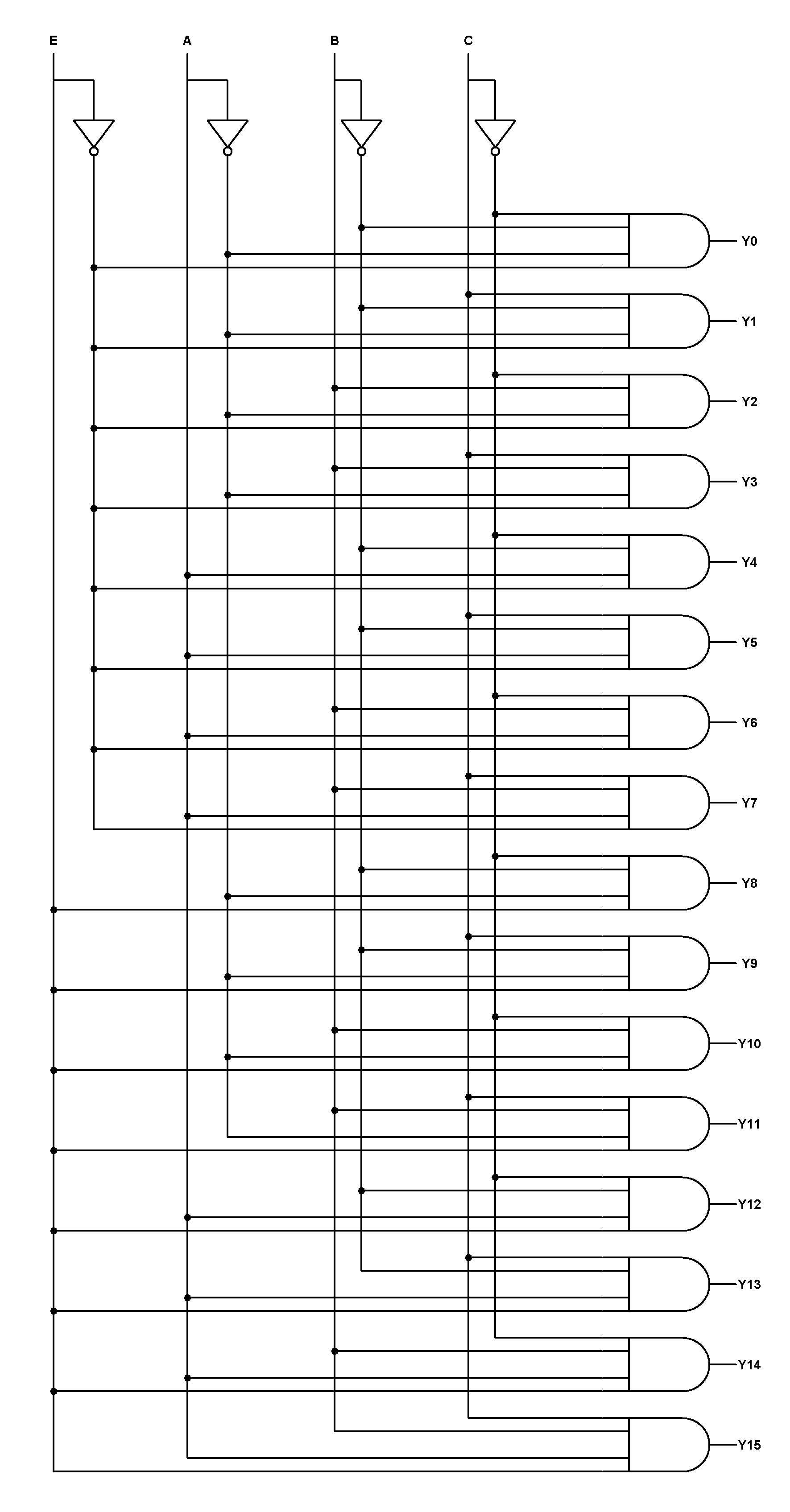
After the completion of laboratory the student will be able to, 1. The only time we use it is to pull it low in order to force q to a logic zero output. Complete the timing diagram (note that. 8x1 mux logic diagram simplified block diagram of the 4 1 multiplexer circuit 1 to 8 demultiplexer plc ladder diagram The logic diagram of the 3 to 8 line decoder is shown below. This information will introduce you to the varied equipment and components you will have to get your. It could possibly on the other hand be confusing to newbies who are just starting out. This is great to create complex logic circuits and can be easily be made into a subcircuit. When the binary input is 0, 1, 2, or 3, the binary output is one greater than the input. Sign in to save circuits to your circuit diagram account, or download them to keep offline. Vhdl code for 1 to 4 demux. Schematic diagram of a circuit. Mux working symbol and logic diagram.